News Posts matching #SOI

Return to Keyword Browsing

UMC Introduces Industry's First 3D IC Solution for RFSOI, Accelerating Innovations in the 5G Era

United Microelectronics Corporation ("UMC"), a leading global semiconductor foundry, today announced the industry's first 3D IC solution for RFSOI technology. Available on UMC's 55 nm RFSOI platform, the stacked silicon technology reduces die size by more than 45% without any degradation of radio frequency (RF) performance, enabling customers to efficiently integrate more RF components to address the greater bandwidth requirements of 5G.

As mobile device manufacturers pack more frequency bands in newer generations of smartphones, the company's 3D IC solution for RFSOI addresses the challenge of integrating more RF front-end modules (RF-FEM) - critical components in devices to transmit and receive data - in a device by vertically stacking dies to reduce surface area. RFSOI is the foundry process used for RF chips such as low noise amplifiers, switches, and antenna tuners. Utilizing wafer-to-wafer bonding technology, UMC's 3D IC solution for RFSOI resolves the common issue of RF interference between stacked dies. The company has received multiple patents for this process, which is now ready for production.

GlobalFoundries and STMicroelectronics Finalize Agreement for 300mm Semiconductor Fab in France

GlobalFoundries Inc., a global leader in feature-rich semiconductor manufacturing, and STMicroelectronics, a global semiconductor leader serving customers across the spectrum of electronics applications, announced today the conclusion of the agreement to create a new, jointly-operated, high-volume semiconductor manufacturing facility in Crolles (France), which was announced on 11 July 2022.

"I would like to thank Minister Le Maire, the French Minister of the Economy and Finance, and his team for their support and the dedication for the last 12+ months that have made celebrating today's milestone possible," said Dr. Thomas Caulfield, President and CEO of GlobalFoundries. "In partnership with ST in Crolles, we are further expanding GF's presence within Europe's dynamic technology ecosystem while benefiting from economies of scale to deliver additional capacity in a highly capital efficient manner. Together we will deliver GF's market leading FDX technology and ST's comprehensive technology roadmap, in alignment with customer demand which is expected to remain high for Automotive, IoT, and Mobile applications over the next decades."

Eliyan Closes $40M Series A Funding Round and Unveils Industry's Highest Performance Chiplet Interconnect Technologies

Eliyan Corporation, credited for the invention of the semiconductor industry's highest-performance and most efficient chiplet interconnect, today announced two major milestones in the commercialization of its technology for multi-die chiplet integration: the close of its Series A $40M funding round, and the successful tapeout of its technology on an industry standard 5-nanometer (nm) process.

Eliyan's NuLink PHY and NuGear technologies address the critical need for a commercially viable approach to enabling high performance and cost-effectiveness in the connection of homogeneous and heterogenous architectures on a standard, organic chip substrate. It has proven to achieve similar bandwidth, power efficiency, and latency as die-to-die implementations using advanced packaging technologies, but without the other drawbacks of specialized approaches.

STMicroelectronics and GlobalFoundries to advance FD-SOI ecosystem with new 300mm manufacturing facility in France

STMicroelectronics, a global semiconductor leader serving customers across the spectrum of electronics applications, and GlobalFoundries Inc., a global leader in feature-rich semiconductor manufacturing, today announced they have signed a Memorandum of Understanding to create a new, jointly-operated 300 mm semiconductor manufacturing facility adjacent to ST's existing 300 mm facility in Crolles, France. This facility is targeted to ramp at full capacity by 2026, with up to 620,000 300 mm wafer per year production at full build-out (~42% ST and ~58% GF).

ST and GF are committed to building capacity for their European and global customer base. This new facility will support several technologies, in particular FD-SOI-based technologies, and will cover multiple variants. This includes GF's market leading FDX technology and ST's comprehensive technology roadmap down to 18 nm, which are expected to remain in high demand for Automotive, IoT, and Mobile applications for the next few decades. FD-SOI technology has origins in the Grenoble (France) area. It has been part of ST technology and product roadmap in its Crolles facility since the early beginnings, and it was later enabled with differentiation and commercialized for manufacturing at GF's Dresden facility. FD-SOI offers substantial benefits for designers and customers, including ultra-low power consumption as well as easier integration of additional features such as RF connectivity, mmWave and security.

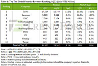
Off-season Offsets Wafer Pricing Increase, 1Q22 Foundry Output Value Up 8.2% QoQ, Says TrendForce

According to TrendForce research, although demand for consumer electronics remains weak, structural growth demand in the semiconductor industry including for servers, high-performance computing, automotive, and industrial equipment has not flagged, becoming a key driver for medium and long term foundry growth. At the same time, due to robust wafer production at higher pricing in 1Q22, quarterly output value hit a new high for the 11th consecutive quarter, reaching US$31.96 billion, 8.2% QoQ, marginally less than the previous quarter. In terms of ranking, the biggest change is Nexchip surpassed Tower at the ninth position.

TSMC's across the board wafer hikes in 4Q21 on batches primarily produced in 1Q22 coupled with sustained strong demand for high-performance computing and better foreign currency exchange rates pushed TSMC's 1Q22 revenue to $17.53 billion, up 11.3% QoQ. Quarterly revenue growth by node was generally around 10% and the 7/6 nm and 16/12 nm processes posted the highest growth rate due to small expansions in production. The only instance of revenue decline came at the 5/4 nm process due to Apple's iPhone 13 entering the off season for production stocking.

GlobalFoundries and STMicroelectronics Considering a New Fab in France

Recent news suggests that TSMC isn't too interested in setting up a fab in Europe, but it appears there are other interested parties that are now courting the EU, namely a potential joint venture between GlobalFoundries and STMicroelectronics. The two companies are hoping to get a slice of the same cake as Intel, namely the European Chips Act, to help subsidise the cost of the proposed fab. Although GlobalFoundries are headquartered in New York and STMicroelectronics in Geneva, the latter being a French-Italian conglomerate, the planned location for the new fab will be somewhere in France.

It's highly unlikely that this will be a cutting edge or even a leading edge fab, as neither company is in the business of producing products in those market segments. ST makes a wide range of chips from MCUs and other types of microprocessors, to specialised memory products, a wide range of sensors, MEMS based devices and all kinds of electronics for electrical vehicles, as well as highly specialised components for the space industry. GloFo obviously stepped off the competitive foundry ladder some years ago and have been focusing on specialised processes and nodes since then, such as FD-SOI, a technology, something the two companies announced a joint partnership around earlier this year. As such, it's likely that this potential fab will focus on making parts needed for the automotive industry in Europe, among other things. There's still a long way to go and neither company has made any kind of official statement about the potential partnership as yet.

UMC is Feeling the Pressure from Chinese Foundries

The chip shortage discussion has been very focused on TSMC for some reason and although the company is without a doubt the world's leading foundry, the company is making its living from being a cutting edge foundry, whereas much of the components that there's a shortage of are made on far older nodes at many different foundries. Taiwanese UMC is one of the foundries that makes many of the automotive semiconductors, as well as key components when it comes to power regulation and is considered the world's third largest foundry.

Until 2018, UMC was competing head on with TSMC, although the company was always about a node behind TSMC, which led to a management team decision to slow down its node transition and instead to focus on speciality technologies. The company has done well in this niche, with a revenue of about US$6.2 billion in 2020. However, UMC is starting to feel the pressure from its competitors in China, as the PRC government is making a push for local production of local IC designs.

Foundry Revenue for 2Q21 Reaches Historical High Once Again with 6% QoQ Growth Thanks to Increased ASP and Persistent Demand, Says TrendForce

The panic buying of chips persisted in 2Q21 owing to factors such as post-pandemic demand, industry-wide shift to 5G telecom technology, geopolitical tensions, and chronic chip shortages, according to TrendForce's latest investigations. Chip demand from ODMs/OEMs remained high, as they were unable to meet shipment targets for various end-products due to the shortage of foundry capacities. In addition, wafers inputted in 1Q21 underwent a price hike and were subsequently outputted in 2Q21. Foundry revenue for the quarter reached US$24.407 billion, representing a 6.2% QoQ increase and yet another record high for the eighth consecutive quarter since 3Q19.

GLOBALFOUNDRIES Announces New 22FDX+ Platform, Extending FDX Leadership with Specialty Solutions for IoT and 5G Mobility

GLOBALFOUNDRIES (GF ), the world's leading specialty foundry, announced today at its Global Technology Conference the next generation of its FDXTM platform, 22FDX+, to meet the ever-growing need for higher performance and ultra-low power requirements of connected devices. GF's industry-leading 22FDX (22 nm FD-SOI) platform has realized $4.5 billion in design wins, with more than 350 million chips shipped to customers around the world.

GF's new 22FDX+ builds on the company's 22FDX platform, offering a broader set of features that provide high performance, ultra-low power, and specialty features and capabilities for the newest generation of designs. The differentiated offering will further empower customers to create chips that are specifically optimized for Internet of Things (IoT), 5G, automotive, and satellite communications applications.

Lattice Semiconductor Announces Certus-NX General Purpose FPGA

Lattice Semiconductor Corporation, the low power programmable leader, today launched the new Lattice Certus -NX family of FPGAs. The devices lead the general-purpose FPGA market in I/O density, delivering up to twice the I/O density per mm2 in comparison to similar competing FPGAs, and provide best-in-class power savings, small size, reliability, instant-on performance, and support fast PCI Express (PCIe) and Gigabit Ethernet interfaces to enable data co-processing, signal bridging, and system control. Certus-NX FPGAs target a range of applications, from data processing in automated industrial equipment to system management in communications infrastructure. The Certus-NX devices are the second family of FPGAs developed on the Lattice Nexus platform, the industry's first low power FPGA platform using 28 nm FD-SOI process technology. With the launch of Certus-NX, Lattice marks the release of the second device family developed under Lattice's new product development strategy in just six months.

"Certus-NX delivers unique and innovative capabilities that set it apart," said Linley Gwennap, Principal Analyst at The Linley Group. "Compared to competing FPGAs of similar gate counts, Lattice offers a much smaller package, greater I/O density, and lower power."

GLOBALFOUNDRIES Delivers Industry's First Production-ready eMRAM on 22FDX Platform

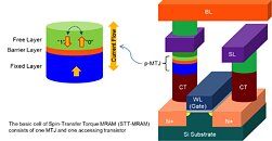
GLOBALFOUNDRIES (GF ) today announced its embedded magnetoresistive non-volatile memory (eMRAM) on the company's 22 nm FD-SOI (22FDX ) platform has entered production, and GF is working with several clients with multiple production tape-outs scheduled in 2020. Today's announcement represents a significant industry milestone, demonstrating the scalability of eMRAM as a cost-effective option at advanced process nodes for Internet of Things (IoT), general-purpose microcontrollers, automotive, edge-AI (Artificial Intelligence), and other low-power applications.

Designed as a replacement for high-volume embedded NOR flash (eFlash), GF's eMRAM allows designers to extend their existing IoT and microcontroller unit architectures to access the power and density benefits of technology nodes below 28 nm.

GLOBALFOUNDRIES and GlobalWafers Sign MOU to Increase Capacity, Supply of 300mm SOI Wafers

GLOBALFOUNDRIES (GF ), the world's leading specialty foundry, and GlobalWafers Co., Ltd. (GWC), one of the top three silicon wafer manufacturers in the world, today announced they have signed a memorandum of understanding (MOU) to develop a long-term supply agreement for 300 mm silicon-on-insulator (SOI) wafers.

GWC is one of the world's leading manufacturers of 200 mm SOI wafers, and has a long and ongoing relationship with GF for supplying 200 mm SOI wafers. GWC also manufactures 300 mm SOI wafers, and under the anticipated supply agreement, GWC and GF will collaborate closely to significantly expand GWC's 300 mm SOI wafer manufacturing capacity.

Samsung Starts Commercial Shipment of eMRAM Based on 28nm FD-SOI

Samsung Electronics Co., Ltd., the world leader in semiconductor technology, today announced that it has commenced mass production of its first commercial embedded magnetic random access memory (eMRAM) product based on the company's 28-nanometer (nm) fully-depleted silicon-on-insulator (FD-SOI) process technology, called 28FDS.

As eFlash has faced scalability challenges due to a charge storage-based operation, eMRAM has been the most promising successor since its resistance-based operation allows strong scalability while also possessing outstanding technical characteristics of memory semiconductors such as nonvolatility, random access, and strong endurance. With today's announcement, Samsung has proved its capability to overcome technical hurdles and demonstrated the possibility for further scalability of embedded memory technology to 28nm process node and beyond.

Samsung Announces Comprehensive Process Roadmap Down to 4 nm

Samsung stands as a technology giant in the industry, with tendrils stretching out towards almost every conceivable area of consumer, prosumer, and professional markets. It is also one of the companies which can actually bring up the fight to Intel when it comes to semiconductor manufacturing, with some analysts predicting the South Korean will dethrone Intel as the top chipmaker in Q2 of this year. Samsung scales from hyper-scale data centers to the internet-of-things, and is set to lead the industry with 8nm, 7nm, 6nm, 5nm, 4nm and 18nm FD-SOI in its newest process technology roadmap. The new Samsung roadmap shows how committed the company is (and the industry with it) towards enabling the highest performance possible from the depleting potential of the silicon medium. The 4 nm "post FinFET" structure process is set to be in risk production by 2020.

This announcement also marks Samsung's reiteration on the usage of EUV (Extreme Ultra Violet) tech towards wafer manufacturing, a technology that has long been hailed as the savior of denser processes, but has been ultimately pushed out of market adoption due to its complexity. Kelvin Low, senior director of foundry marketing at Samsung, said that the "magic number" for productivity (as in, with a sustainable investment/return ratio) with EUV is 1,500 wafers per day. Samsung has already exceeded 1,000 wafers per day and has a high degree of confidence that 1,500 wafers per day is achievable.

GlobalFoundries Announces its 12 nm FD-SOI Silicon Fabrication Node

GLOBALFOUNDRIES today unveiled a new 12nm FD-SOI semiconductor technology, extending its leadership position by offering the industry's first multi-node FD-SOI roadmap. Building on the success of its 22FDXTM offering, the company's next-generation 12FDXTM platform is designed to enable the intelligent systems of tomorrow across a range of applications, from mobile computing and 5G connectivity to artificial intelligence and autonomous vehicles.

As the world becomes more and more integrated through billions of connected devices, many emerging applications demand a new approach to semiconductor innovation. The chips that make these applications possible are evolving into mini-systems, with increased integration of intelligent components including wireless connectivity, non-volatile memory, and power management-all while driving ultra-low power consumption. GLOBALFOUNDRIES' new 12FDX technology is specifically architected to deliver these unprecedented levels of system integration, design flexibility, and power scaling.

Cadence Announces Tapeout of 14 nm Test-Chip

Cadence Design Systems, Inc., a leader in global electronic design innovation, announced today the tapeout of a 14-nanometer test-chip featuring an ARM Cortex-M0 processor implemented using IBM's FinFET process technology. The successful tapeout is the result of close collaboration between the three technology leaders as they teamed to build an ecosystem to address the new challenges from design through manufacturing inherent in a 14-nanometer FinFET-based design flow.

The 14-nanometer ecosystem and chip are significant milestones of a multi-year agreement between ARM, Cadence and IBM to develop systems-on-chip (SoCs) at the advanced process nodes of 14 nanometers and beyond. SoCs designed at 14 nanometers with FinFET technology offer the promise of a significant reduction in power consumption.

Common Platform Transitions to Adopt FinFET 3D Transistor with 14 nm Fab Process

Common Platform, a consortium of three major silicon fabrication companies: IBM, Samsung, and GlobalFoundries, met at their 2012 Technology Forum, where they announced their intention to transition to FinFET 3D transistor technology, but only with the 14 nanometer (nm) silicon fabrication process. Chips on this process will be built in the 2014~2015 time-frame. 3D transistors is a technology pioneered by Intel, which provides space-optimized, energy-efficient transistors on a nano-scale.

FinFET transistors will be combined with Fully Depleted Silicon-On-Insulator (FD-SOI) to offer extremely high transistor densities, with lower chip power. FD-SOI overcomes the limitation of current partially-depleted SOI (PD-SOI) technology, of lower-yields due to the pressure required for SOI insulation, which nears the breaking-point of strained silicon transistors. FinFET tech will be combined with chip-stacking technology, which helps make devices with better use of available PCB footprint.

IBM Microprocessors to Power the New Wii U System from Nintendo

IBM today announced that it will provide the microprocessors that will serve as the heart of the new Wii U system from Nintendo. Unveiled today at the E3 trade show, Nintendo plans for its new console to hit store shelves in 2012.

The all-new, Power-based microprocessor will pack some of IBM's most advanced technology into an energy-saving silicon package that will power Nintendo's brand new entertainment experience for consumers worldwide. IBM's unique embedded DRAM, for example, is capable of feeding the multi-core processor large chunks of data to make for a smooth entertainment experience.

New Intel Atom Processor Platform Significantly Lowers Power for Tablet and Handheld

Benefitting from the company's power-saving architecture, transistor and circuit design expertise, plus unique manufacturing process techniques, Intel Corporation today unveiled its newest Intel Atom processor-based platform (formerly "Moorestown").

The technology package provides significantly lower power consumption and prepares the company to target a range of computing devices, including high-end smartphones, tablets and other mobile handheld products. The chips bring Intel's classic product strengths - outstanding performance to run a comprehensive and growing number of rich media and Internet applications, a choice of software, and the ability to easily multitask - across a number of applications, including HD video and multi-point videoconferencing.

GLOBALFOUNDRIES To Highlight 32nm/28nm Technology Leadership at GSA Expo

As the semiconductor industry begins its transition to the next technology node, GLOBALFOUNDRIES is on track to take its position as the foundry technology leader. On October 1 at the Global Semiconductor Alliance Emerging Opportunities Expo & Conference in Santa Clara, Calif., GLOBALFOUNDRIES (Booth 321) will provide the latest details on its technology roadmap for the 32nm/28nm generations and its innovative "Gate First" approach to building transistors based on High-K Metal Gate (HKMG) technology.

"With each new technology generation, semiconductor foundries are increasingly challenged with the economics to sustain R&D and the know-how to bring these technologies to market in high-volume," said Len Jelinek, director and chief analyst, iSuppli. "With a heritage of rapidly ramping leading-edge technologies to high volumes at mature yields, combined with aggressive investments in capacity and technology, GLOBALFOUNDRIES is uniquely-positioned to challenge for next-generation foundry leadership."

AMD Demos 48-core ''Magny-Cours'' System, Details Architecture

Earlier slated coarsely for 2010, AMD fine-tuned the expected release time-frame of its 12-core "Magny-Cours" Opteron processors to be within Q1 2010. The company seems to be ready with the processors, and has demonstrated a 4 socket, 48 core machine based on these processors. Magny Cours holds symbolism in being one of the last processor designs by AMD before it moves over to "Bulldozer", the next processor design by AMD built from ground-up. Its release will provide competition to Intel's multi-core processors available at that point.

AMD's Pat Conway at the IEEE Hot Chips 21 conference presented the Magny-Cours design that include several key design changes that boost parallelism and efficiency in a high-density computing environment. Key features include: Move to socket G34 (from socket-F), 12-cores, use of a multi-chip module (MCM) package to house two 6-core dies (nodes), quad-channel DDR3 memory interface, and HyperTransport 3 6.4 GT/s with redesigned multi-node topologies. Let's put some of these under the watch-glass.

Power-Shift in Fab 36 Dresden, New Fab to Take Third-Party Orders

After a successful shareholder approval AMD received for spinning-off its manufacturing division to form The Foundry Company (TFC) with a majority stake holding by Advanced Technology Investment Company (ATIC), top-brass of the Fab subsidiary in Dresden, German saw a power-shift. Long-standing general manager Hans Deppe left the company, to be succeeded by Jim Doran.

Doran's experience with the subsidiary covering Fab 36 (65 nm SOI capable) and Fab 38 (45 nm SOI capable) includes being its general manager in the past, which made with a contender to the post. The Dresden facilities will officially come under TFC from March 2. While as part of AMD the facilities were dedicated to manufacturing AMD microprocessor parts, under TFC, not only will they serve as foundry-partner for AMD, but also accept designs from other companies seeking manufacture on the facilities TFC offers.

NVIDIA Joins SOI Consortium

The SOI Industry Consortium has announced that NVIDIA has joined the organization. NVIDIA now joins a league of companies such as AMD, Applied Materials, ARM, Cadence Design Systems, CEA-Léti, Chartered Semiconductor Manufacturing, Freescale Semiconductor, IBM, Innovative Silicon, KLA-Tencor, Lam Research, Magma Design, Samsung, Semico, Soitec, SEH Europe, STMicroelectronics, Synopsys, Taiwan Semiconductor Manufacturing Company (TSMC), Tyndall Institute, UCL and United Microelectronics Corporation (UMC).

So what is SOI? Silicon on Insulator technology involves use of variable layered silicon-insulator-silicon substratum, used to minimize parasitic device capacitance and thereby improve performance.
Return to Keyword Browsing
Jun 1st, 2024 22:51 EDT change timezone

New Forum Posts

Popular Reviews

Controversial News Posts