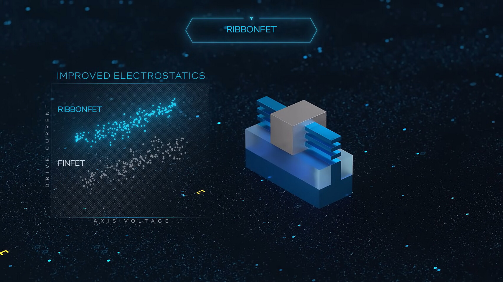
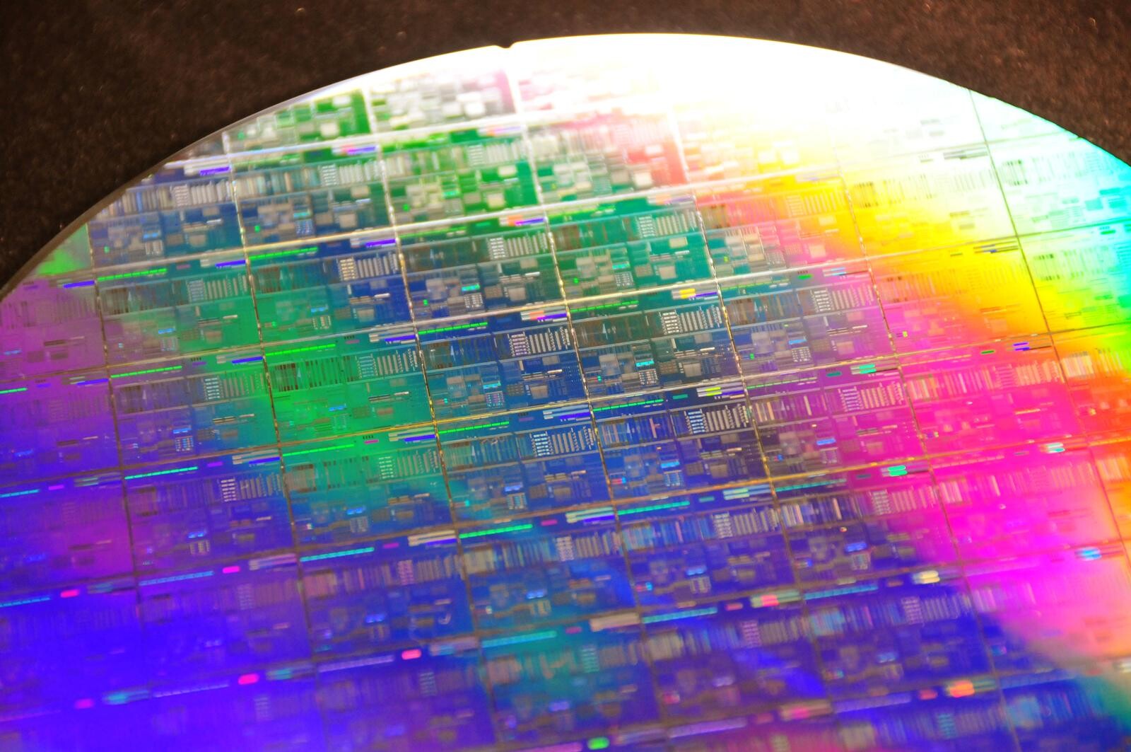
DNP Develops Photomask Process for 3nm EUV Lithography
Dai Nippon Printing Co., Ltd. (DNP) has successfully developed a photomask manufacturing process capable of accommodating the 3-nanometer (10-9 meter) lithography process that supports Extreme Ultra-Violet (EUV) lithography, the cutting-edge process for semiconductor manufacturing.
Background
DNP has continually responded to the demands of semiconductor manufacturers in terms of performance and quality. In 2016, we became the world's first merchant photomask manufacturer to introduce the multi-beam mask writing tool (MBMW). In 2020, we developed a photomask manufacturing process for 5 nm EUV lithography processes, and have been supplying masks that meet the needs of the semiconductor market. In this latest development, in order to meet the needs of further miniaturization, we have developed a photomask for EUV lithography capable of supporting 3 nm processes.