Report an Error

Intel Tiger Lake GT2
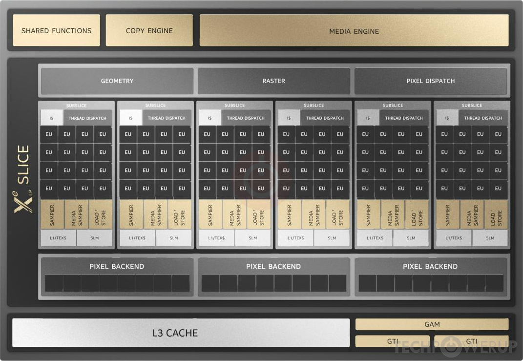
Block Diagram
Intel's Tiger Lake GT2 GPU uses the Generation 12.1 architecture and is made using a 10 nm production process at Intel. With a die size of 146 mm² it is a small chip. Tiger Lake GT2 supports DirectX 12 (Feature Level 12_1). For GPU compute applications, OpenCL version 3.0 can be used. It features 768 shading units, 48 texture mapping units and 24 ROPs.
Graphics Processor
- Released
- Sep 2nd, 2020
- GPU Name
- Tiger Lake GT2
- Architecture
- Generation 12.1
- Foundry
- Intel
- Process Size
- 10 nm
- Transistors
- unknown
- Die Size
- 146 mm²
- Package
- FCBGA-1449/1598
Graphics Features
- DirectX
- 12 (12_1)
- OpenGL
- 4.6
- OpenCL
- 3.0
- Vulkan
- 1.3
- Shader Model
- 6.6
- WDDM
- 3.1
Render Config
- Shading Units
- 768
- TMUs
- 48
- ROPs
- 24
- Execution Units
- 96
- FP16 Units
- 1536
- FP64 Units
- 192
- Subslices
- 6
- Slices
- 1
- L2 Cache
- 1024 KB
- L3 Cache
- 3.75 MB
- Max. TDP
- 15 W
All Generation 12.1 GPUs
- Intel DG1
- Intel Rocket Lake GT1
- Intel Tiger Lake GT1
- Intel Tiger Lake GT2
Intel GPU Architecture History
- 2023 Xe-LPG
- 2022-2023 Generation 12.7
- 2021-2024 Generation 12.5
- 2021-2023 Generation 12.2
- 2020-2021 Generation 12.1
- 2019-2021 Generation 11.0
- 2016-2020 Generation 9.5
- 2015-2016 Generation 9.0
- 2014-2015 Generation 8.0
- 2013 Generation 7.5
- 2012-2013 Generation 7.0
- 2011 Generation 6.0
- 2010-2013 Knights
- 2010 Generation 5.75
- 2008-2010 PowerVR SGX545
- 2008 Generation 5.0
- 2008-2010 PowerVR SGX535
- 2006-2007 Generation 4.0
- 2005-2006 Generation 3.5
- 2004-2005 Generation 3.0
- 2002-2003 Generation 2.0
- 1998 i740
- 1998-2002 Generation 1.0
Graphics cards using the Intel Tiger Lake GT2 GPU
| Name | Chip | Memory | Shaders | TMUs | ROPs | Base Clock | Boost Clock | Memory Clock |
|---|---|---|---|---|---|---|---|---|
| System Shared | 768 | 48 | 24 | 300 MHz | 1100 MHz | System Shared | ||
| System Shared | 640 | 40 | 20 | 300 MHz | 1100 MHz | System Shared | ||
| System Shared | 384 | 24 | 12 | 300 MHz | 1100 MHz | System Shared |
Jun 2nd, 2024 00:14 EDT
change timezone
Latest GPU Drivers
New Forum Posts
- Last game you purchased? (314)
- Oddballz eggs used to be on the internet (2)
- What system around 2070 super FTW3 ultra 8GB? (9)
- 3D/Game Design Workstation (11)
- Dude, youre hotrodding a Dell... (2)
- Would you pay more for hardware with AI capabilities? (88)
- Overclock AMD Ryzen 9 5900X On ROG STRIX B550-A GAMING After New Bios Update. (29)
- how can i install intel dc ssd p3600 ??? (2)
- Flash original BIOS - Asrock RX570 (0)
- SSD cooling advice (12)
Popular Reviews
- SilverStone KL07E Review
- ID-Cooling FX360 PRO Review - Shots Fired @ Arctic
- NuPhy Air96 V2 Low Profile Wireless Mechanical Keyboard Review
- Upcoming Hardware Launches 2024 (Updated May 2024)
- Montech Titan Gold 1000 W Review
- Elysian Acoustic Labs Pilgrim In-Ear Monitors Review
- Senua’s Saga: Hellblade II: DLSS vs. FSR vs. XeSS Comparison Review
- Ghost of Tsushima Performance Benchmark Review - 35 GPUs Tested
- Senua's Saga: Hellblade II Performance Benchmark Review
- AMD Ryzen 7 7800X3D Review - The Best Gaming CPU
Controversial News Posts
- AMD to Redesign Ray Tracing Hardware on RDNA 4 (227)
- NVIDIA to Only Launch the Flagship GeForce RTX 5090 in 2024, Rest of the Series in 2025 (154)
- AMD Hits Highest-Ever x86 CPU Market Share in Q1 2024 Across Desktop and Server (140)
- AMD RDNA 5 a "Clean Sheet" Graphics Architecture, RDNA 4 Merely Corrects a Bug Over RDNA 3 (139)
- NVIDIA RTX 5090 "Blackwell" Founders Edition to Implement the "RTX 4090 Ti" Cinderblock Design (118)
- Core Configurations of Intel Core Ultra 200 "Arrow Lake-S" Desktop Processors Surface (101)
- Biden Administration to Revive Trump-Era Tariffs on China-made GPUs and Motherboards (95)
- AMD Ryzen 9000 Zen 5 Single Thread Performance at 5.80 GHz Found 19% Over Zen 4 (87)